 by
by
× nearby
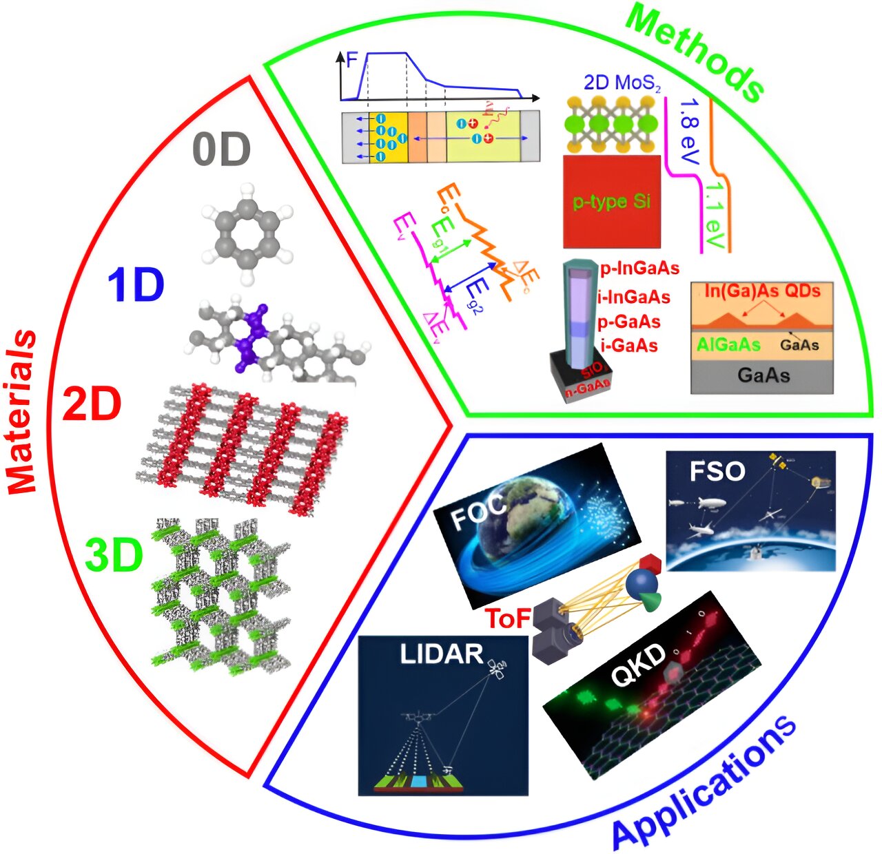
Methods, materials and applications of avalanche photon-sensing technologies ranging from bulk to low-density materials. Credit: Light: Science and Applications (2023). DOI: 10.1038/s41377-023-01259-3
The result of the avalanche frequency can be used to detect low power signals and single photons due to the amplification device among all the main ranges: near- (NIR), short- (SWIR), mid- (MWIR) and long-wave infrared radiation. (LWIR). Sophisticated laser radar and weapon systems implemented in long-range military and space applications must detect, recognize and track various targets under various atmospheric conditions including absorption by CO, CO.2 and H2O smoke, which leads to a decrease in the vital signal in the eye system.
Such compression of the output signal requires an additional amplifier and a system to accurately detect the signal at the detector level. Devices based on avalanche photodiodes (APDs) showing high bandwidth (BW) and gain (M) in the production of high gain bandwidth (GBW) and low noise. [F(M)] at the same time it is well suited to the detection of compressed optical signals, for example, in long-range applications such as free-space optical communications (FSO), night vision, light detection and tracking (LIDAR / LADAR), time of travel. (ToF), intelligent robots and finally in battle situations (military applications).
The main reason for this trend is undoubtedly the move to applications of optical quantum information such as quantum key distribution (QKD). Such applications place strict demands on the performance of the detector that separates from the performance of conventionally established APDs. Therefore, improving GBW and reducing F(M) has been the main goal of APD development.
F(M) compression techniques can be divided into three techniques. The first way would be to choose materials (including “third wave” materials and their technologies) with beneficial replication properties. Next, F(M) can be greatly reduced by burning the avalanche layer to use the non-local effect of the multiplicative effect. The latter approach can be broadly classified as impact ionization engineering (I2E) using properly designed heterojunctions.
A member of the group of “third waves” – 2-dimensional (2D) charged materials and their van der Waals (vdW) heterostructures can also be used in the field of avalanche multiplication to include single-photon counting techniques. The last decade has seen a dramatic growth in the number of research papers related to promising 2D photodetectors, however, those devices show low absorption caused by the thin nature of the atom. Impact ionization leading to carrier multiplication is a promising method to fabricate 2D photodetectors with high efficiency.
Compared to conventional bulk, 2D devices show many unique capabilities, such as mechanical flexibility, strong light coupling, moving parts and the Fermi level that provide flexibility in heterostructure design. Those materials are characterized by ionization coefficients of different effects against the direction of carrier transport. In addition, not only the general ionization effect but also the ballistic avalanche mechanism was observed in the family of 2D instruments.
As a result, the research of new materials characterized by a low electrical frequency avalanche is important to achieve efficient electrical/electrical devices. The method of avalanche replication in conventional materials is limited due to the high driving voltage that can be generated by 2D materials based APDs.
In a new paper published in Light: Science and Applications, a group of scientists, led by Professor Piotr Martyniuk from the Institute of Applied Physics, Military University of Technology, Poland and authors from the State Key Laboratory of Infrared Physics, Shanghai Institute of Technical Physics, Chinese Academy of Sciences , China has now shown. status and future developments in IR-based APDs. This paper includes both HgCdTe and AIIIBV systems based on HgCdTe and AIIIBV which includes the well-known “third wave” member of the material family-superlattices.
In addition, current progress in new materials and designs for high-performance IR APDs was shown to include “third wave” 2D materials, and strategies to achieve high-performance APDs were presented.
More information:
Piotr Martyniuk et al, Infrared avalanche photodiodes from bulk to 2D devices, Light: Science and Applications (2023). DOI: 10.1038/s41377-023-01259-3
Journal information:
Light: Science and Applications
#Infrared #avalanche #photodiodes #bulk #materials